-
E-mail
huahui@shchylyqyxgs.wecom.work
-
Phone
15026706579
-
Address
No. 115, Lane 1276, Nanle Road, Songjiang District, Shanghai
Shanghai Chaohui Pressure Instrument Co., Ltd
Application of Ultrasonic Scanning Microscope
Date: 2025-11-06Read: 71
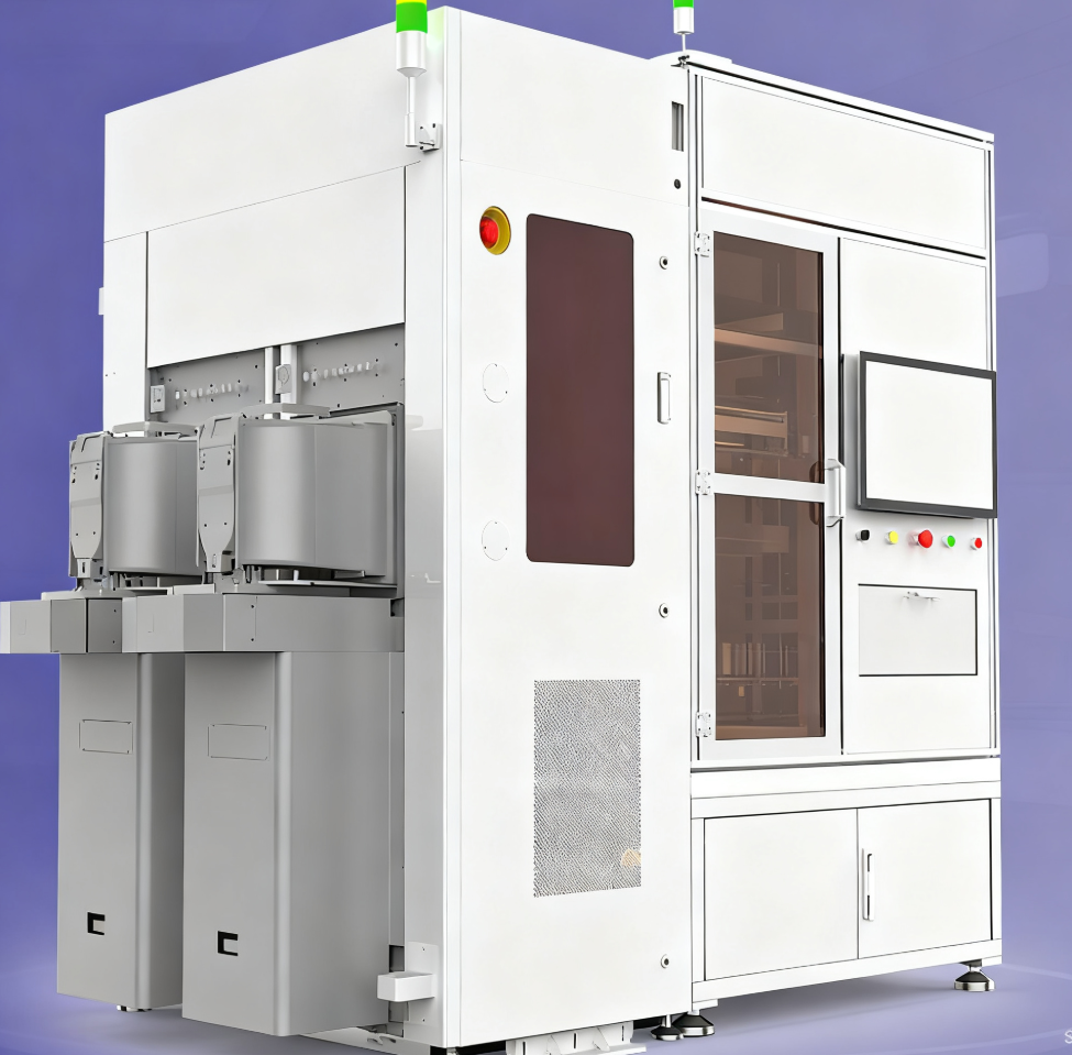
Ultrasonic scanning microscope is a highly practical toolNon destructive testing tools. This product mainly uses high-frequency ultrasound to detect various semiconductor devices and materials, and can detect defects such as pores, cracks, inclusions, and delamination inside the sample, and visually display them in the form of graphics. During the scanning process, it will not cause damage to the sample and will not affect its performance. Therefore, it is widely used in semiconductor device and packaging testing, material testing, IGBT power module product testing and other occasions.
Supports scanning modes such as A, B, C scanning, transmission scanning, multi-layer scanning, JEDEC tray scanning, thickness measurement, etc. Display the location, shape, and size of internal defects in the tested part in the form of images, and perform size and area statistics of the defects, automatically calculating the percentage of defects in the measured area.
Application fields:
Semiconductor device and packaging testing:
Discrete devices (IGBT/SiC), ceramic substrates, encapsulated ICs, optoelectronic devices, microwave power devices, MEMS devices, flip chip, stacked die, MCM multi chip modules, etc.
Material testing:
Ceramics, glass, metal, plastic, welded parts, water-cooled radiators, etc.
IGBT power module product testing:
Realize non-destructive testing of internal interfaces and structural defects in IGBT modules, accurately identify problems in IGBT module materials and processes, screen for non-conforming products, and promote the improvement of IGBT module packaging quality.
Core technical features
Multi parameter synchronous acquisition: Simultaneously obtaining multiple key parameters such as amplitude, phase, sound velocity, attenuation coefficient, etc. of ultrasound, which is more comprehensive than single parameter detection.
High resolution imaging: By using high-frequency ultrasound (usually in the MHz GHz range), it is possible to achieve micrometer or even nanometer level resolution and clearly present microstructures.
Non destructive testing characteristics: Ultrasonic signals have strong penetrability and do not require sample destruction, making them suitable for internal testing of solid materials (metals, semiconductors, composite materials, etc.).
Main application scenarios
In the field of electronic manufacturing: detecting internal voids, cracks, bonding defects in semiconductor chips and packages, as well as delamination issues in PCB boards.
In the field of materials science: analyzing the internal structural uniformity and porosity of composite materials, as well as detecting small cracks and inclusions in metal materials.
In the field of industrial quality inspection, internal quality screening is conducted on precision mechanical parts, battery electrodes, transformer insulation components, etc. to ensure product reliability.
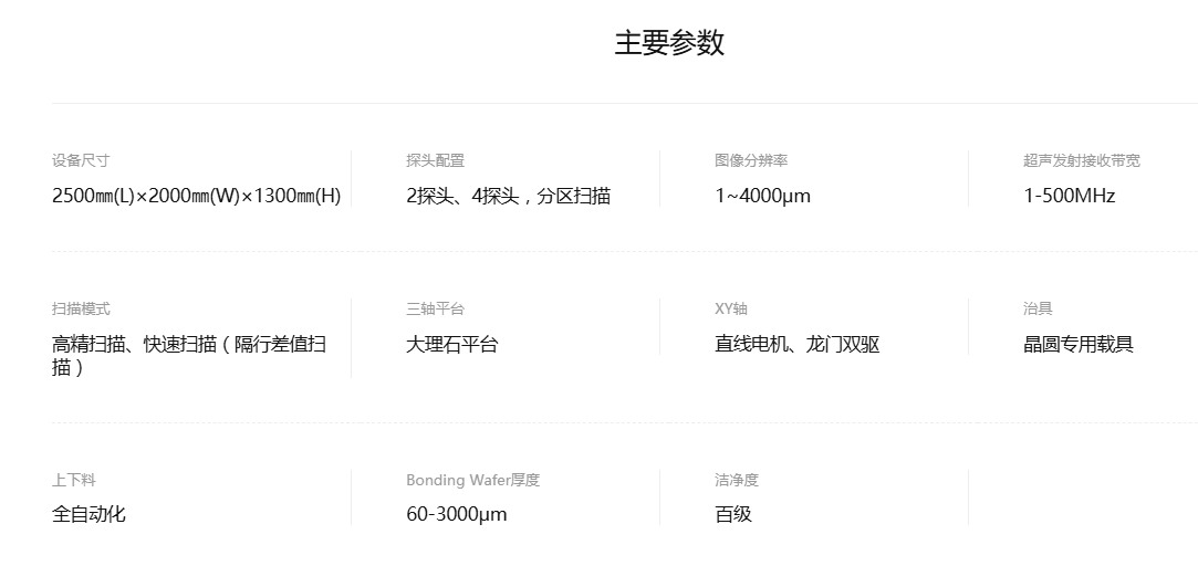
Key performance indicators
Scanning range: ranging from a few millimeters to tens of centimeters, suitable for different sizes of sample detection needs.
Detection depth: Depending on the sample material and ultrasonic frequency, the depth ranges from micrometers to centimeters. High frequency is suitable for shallow microscopic detection, while low frequency is suitable for deep penetration.
Imaging speed: Supports high-speed scanning mode, combined with algorithm optimization, to meet the needs of batch detection or rapid analysis.