-
E-mail
huangyurong@szskyan.com
-
Phone
13316818270
-
Address
2203B, Building A, Xinghe WORLD, Wuhe Avenue, Longgang District, Shenzhen
Shenzhen Century Tianyuan Instrument Co., Ltd
Introduction to Bruker Optical Profilometer (White Light Interferometer) Products and Applications
Date: 2025-12-15Read: 10
Brook(User)Optical profiler(white light interferometer)Product and Application Introduction
1Product Line Introduction:
Brook(User)It is the ***** solution for 3D surface metrology and detection, providing a fast, reliable, and easy-to-use non-contact 3D contour characterization solution. Samples as small as the microscopic field of viewMEMSStructure, large to complete mechanical engine. These solutions provide researchers and engineers in R&D, manufacturing, and quality control with the industry's highest sensitivity and stability. And this is precisely the challenge faced by other metrology methods in the application of fine 3D surface measurement.
Brooke's optical profiler is based onWyko ®Our proprietary core technology, accumulated over ten generations, provides high precision and stability that other measurement systems cannot match. Today, these are becoming the mainstream application scenarios for precision surface 3D measurement. Our measurement tools have been proven to support research and discovery in both laboratory and production environments,The equipment is widely used in industries such as semiconductors and optics.
Brooke's optical profilometer includes the following models: Desktop SeriesContourX-100,X-200,X-500The floor standing seriesContourX-1000,NPFLEX-1000, as well as specifically designed forPCBPanel designContourSP, as well as for surface analysis in the field of data storageHD9800+.
IIFeature Introduction:
Brooke's 3D optical profilometerKnown for non-contact, high precision, and high adaptability,Can provide micro level support for research and development, quality control, and online production MEMSStructure to the whole piece300 mm3D surface measurement solution for wafers and even larger sized partsThe main functions are listed below.
1High precision measurement of surface morphology:<0.01nmThe surface resolution,<0.1%The height repeatability of the steps.

2Traceable results that meet standards: As a measuring device, the Brooke 3D optical profilometer is extremely accurate in measuring height.
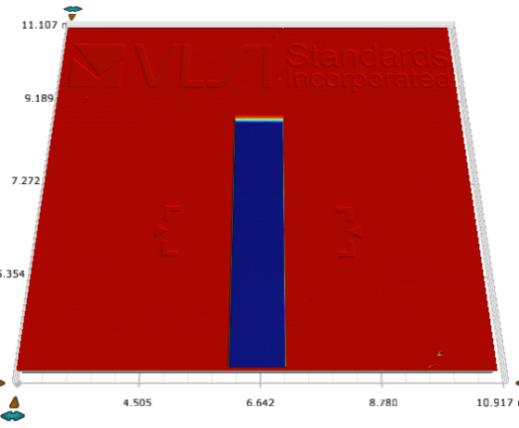
3Universal measurement mode: automatically recognizes surface textures and optimizes signals, balancing sub nanometer accuracy and large step height.
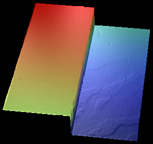
4EliteEnhanced imaging: providing high fidelity while maintaining measurement accuracy2DOptical images.
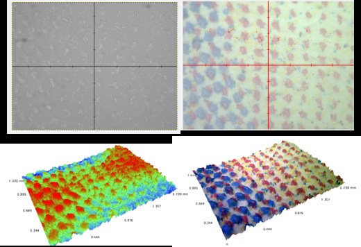
5tilt/Pitch optical head: Specific models achieve constant measurement and focusing position when tilting the side head, greatly improving testing efficiency and usability.

6Efficient analysis software: thousands of preset filters and analysis scripts, one click outputISO25178TheASME B46.1Waiting for the prescribed standard parameters.

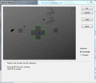
7Automatic batch processing: autofocus, automatic lighting, coordinate file import, pattern recognition, and moreESDProtection, achieving "one click" batch measurement.
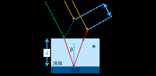
8Film thickness measurement mode: By measuring the reflected signals on the upper and lower surfaces of the transparent film, the film thickness of the thin film is calculated.
IIIApplication Introduction:
1precision machiningThe metrological measurement system accurately and efficiently measures the three-dimensional dimensions of precision machined surface quality or micro nano machining patterns, providing sufficient feedback and reporting for monitoring, tracking, and process evaluation, greatly improving process development efficiency.
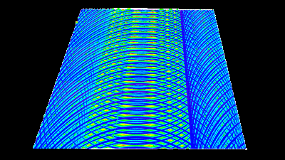
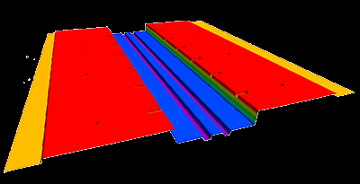
2Micro electromechanical systems and sensorsProvide high-throughput and high repeatability measurements of etching depth, film thickness, step height, and surface roughness to provide accurate and efficient support for process monitoring.
3****Accurate and reproducible measurements are taken on various surfaces of implanted materials and components to provide quality assurance.
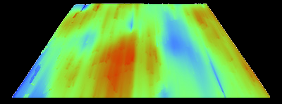
4friction and wearQuantitative measurement of volumetric wear, accurate analysis and evaluation of friction, wear, lubrication, and corrosion on materials/The impact on the performance and lifespan of components.
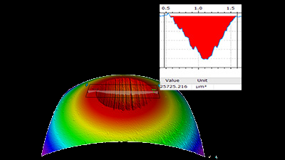
5semiconductorMeasure roughness and flatness; Height, coplanarity, and defect identification and analysis of convex blocks; And key three-dimensional dimension measurements of various structures such as lines, holes, and film layers. For example, rewiring in the field of packaging(RDL)Three dimensional stacked silicon perforation(TSV)Three dimensional monitoring of processes such as carrier boards.
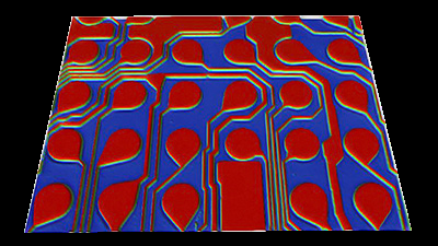
6. OpticsAccurately and repetitively measure the surface of optical materials and components, quantitatively evaluate defects, and help optimize the machining process. For example, monitoring the surface quality of various optical planes and surfaces, as well as automatic measurement of micro nano optical structures (period, depth, etc.) and micro lens arrays (diameter, curvature, vector, etc.).