-
E-mail
sales@chotest.com
-
Phone
18928463988
-
Address
No. 1001, Xili Xueyuan Avenue, Nanshan District, Shenzhen, China
Shenzhen Zhongtu Instrument Co., Ltd
Brand of thin film stair step tester
- Model
- Nature of the Manufacturer
- Producers
- Product Category
- Place of Origin
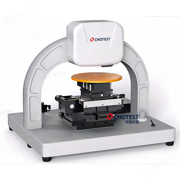
Zhongtu Instrument NS SeriesBrand of thin film stair step testerWith sub angstrom level accuracy, multi scenario adaptability, and intelligent operation, it can accurately measure step height (nanometer to 1050 μ m), surface roughness (parameters such as Ra and Rz), film thickness, and stress distribution, providing reliable data support for material research and development, process optimization, and quality control.
1、 Product Features
1. Parameter measurement function
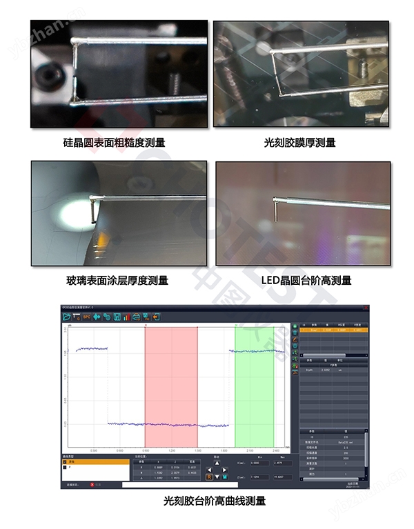
(1) Step height: capable of measuring step heights from nanometers to 330 μ m or 1050 μ m, accurately measuring etching, sputtering SIMS、 Materials deposited or removed during processes such as deposition, spin coating, CMP, etc.
(2) Roughness and waviness: It can measure the roughness and waviness of the sample. The analysis software can obtain dozens of parameters related to roughness and waviness, such as Ra, RMS, Rv, Rp, Rz, etc., by calculating the micro profile curve scanned.
(3) Stress measurement: It can measure the surface stress of various materials.
2. Measurement mode and analysis function
(1) Single area measurement mode: After completing Focus, set the scanning starting point and scanning length according to the image navigation map to start measurement.
(2) Multi area measurement mode: After completing Focus, set up a single area scanning path based on the image navigation map. Multiple area measurement modes can be formed by arranging several to tens of hundreds of scanning paths based on horizontal and vertical distances, and automatic measurement of all scanning paths can be completed with just one click.
(3) 3D measurement mode: After completing Focus, the single area scanning path can be set according to the image navigation map, and the entire scanning area can be set according to the required scanning area width or the spacing and quantity of scanning lines. One click can automatically complete the scanning and 3D image reconstruction of the entire scanning area.
(4) SPC statistical analysis: supports the analysis of multiple indicator parameters for different types of tested parts, and provides SPC charts for measuring data of batch samples to statistically analyze the trend of data changes.
3. Dual navigation optical imaging function
The NS200-D model is equipped with a 500W pixel color camera for both frontal and oblique views. The scanning path can be accurately set in the frontal navigation imaging system, and the scanning trajectory can be tracked in real-time in the oblique navigation imaging system.
4. Quick needle change function
The magnetic probe is used, and when a needle replacement operation is required, the scanning probe can be quickly replaced on site and quickly calibrated according to the calibration module in the software to ensure accuracy and repeatability after needle replacement, reducing maintenance troubles.

2、 Application Fields
NS seriesBrand of thin film stair step testerIt has strong adaptability to application scenarios and does not have special requirements for the reflectivity characteristics, material types, and hardness of the tested samples. It can be widely used in various industries such as semiconductors, solar photovoltaics, optical processing, LED, MEMS devices, micro nano material preparation, and other industrial enterprises and research institutions such as universities. Its accurate characterization of surface micro morphology parameters is of great significance for the evaluation of related materials, performance analysis, and improvement of processing technology.
3、 Application scenarios
1. Semiconductor manufacturing: measurement of deposition/etching film thickness, CMP process flatness detection, analysis of resist step height, to help improve chip yield.
2. Photovoltaic&Display Panel: Measurement of solar coating film thickness, analysis of AMOLED screen microstructure, measurement of copper traces on touch panels, suitable for the production needs of photovoltaic modules and display devices.
3. MEMS&Micro Nano Materials: Micro sensor morphology characterization, flexible electronic film thickness detection, supporting the research and mass production quality control of micro nano devices.
4. Research and universities: Material surface stress analysis, microfabrication technology research and development data support, accelerate the landing of scientific research projects.
4、 Usage environment
Relative humidity: humidity (non condensing) 30-40% RH
Temperature: 16-25 ℃ (with a temperature change of less than 2 ℃ per hour)
Ground vibration: 6.35 μ m/s (1-100Hz)
Audio noise: ≤ 80dB
Air laminar flow: ≤ 0.508 m/s (downward flow)
If you need to customize measurement solutions, obtain detailed parameters, or apply for sample testing for your industry scenario, please feel free to contact Zhongtu Instrument at any time. We will provide you with professional technical support and consulting services!
(Note: Product parameters and functions may be updated with technological upgrades, subject to actual communication)


