-
E-mail
sales@chotest.com
-
Phone
18928463988
-
Address
No. 1001, Xili Xueyuan Avenue, Nanshan District, Shenzhen, China
Product Categories
Shenzhen Zhongtu Instrument Co., Ltd


Graphless wafer thickness measurement system
NegotiableUpdate on 11/19
- Model
- Nature of the Manufacturer
- Producers
- Product Category
- Place of Origin
Overview
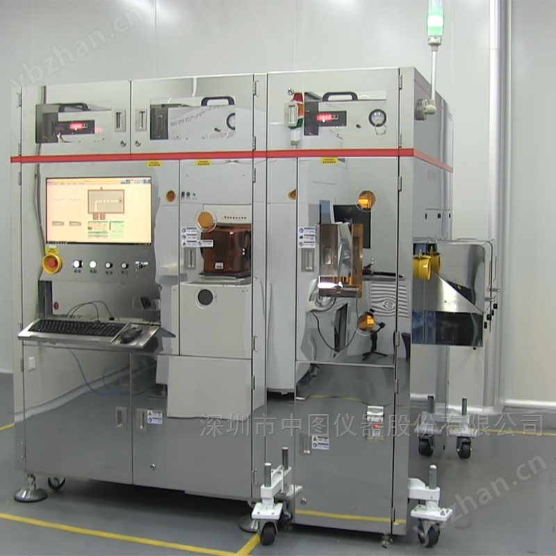
The WD4000 non image wafer thickness measurement system is equipped with one device for measuring thickness, 3D morphology, and roughness parameters. It is used in ultra precision processing fields such as substrate manufacturing, wafer manufacturing, packaging process testing, 3C electronic glass screens and precision accessories, optical processing, display panels, MEMS devices, etc.
Product Details
Zhongtu Instrument WD4000Graphless wafer thickness measurement systemOne device can handle full parameter measurement of thickness, 3D morphology, and roughness, bidding farewell to the tedious coordination of multiple devices, balancing high precision and efficiency, and adapting to the ultra precision testing needs of multiple industries.

1、 Product advantages
1. High precision measurement, reliable data
(1) Spectral confocal imaging technology+white light interferometry technology, Z-direction resolution of 0.1nm, sub nanometer level local height measurement, meeting the requirements of nanometer to micrometer level workpiece detection.
(2) Supports over 300 parameter evaluations for the four major standards of SEMI/ISO/ASME/EUR/GBT, with traceable measurement results.
2. Large stroke high-speed, suitable for multiple specifications of workpieces
(1) 400x400x75mm large stroke gantry structure, with a maximum moving speed of 500mm/s, doubling the detection efficiency.
(2) Compatible with up to 12 inch wafers, paired with electrostatic discharge coating vacuum suction cups, suitable for various surface workpieces such as smooth/rough, low/high reflectivity, etc.
3. Stable anti-interference, worry free operation
(1) Granite pedestal+vibration isolation design, resistant to ground and acoustic vibrations, with excellent measurement repeatability.
(2) Double collision avoidance+electric objective lens switching+XYZ joystick, simplifying the operation process, reducing the risk of misoperation, and reducing training costs.
4. Intelligent automation, adapted to industrial assembly lines
(1) Mapping tracking technology+machine vision Mark point positioning, supports automatic measurement of multiple points, lines, and surfaces, and CNC mode compatible with barcode scanner input.
(2) Virtual fixtures can be used to straighten samples and achieve continuous automated detection of multi-point morphology, suitable for mass production scenarios.

2、 Core functions
1. Non contact measurement: Avoid scratching the surface of precision workpieces such as silicon carbide, sapphire, and silicon, and protect the integrity of the tested object.
2. Integrated design: No need to switch multiple devices, synchronously complete thickness TTV、LTV、BOW、WARP、 Measurement of roughness and three-dimensional morphology, saving space and investment costs.
3. Complete process integration of measurement software function data management, analysis, and integration:
(1) Full functional measurement and analysis
① Covering core measurement requirements such as thickness, 3D morphology, roughness, geometric contour, etc., supporting feature measurement such as step height, angle, curvature, and shape tolerance evaluation.
② Built in five analysis modules, including ISO standard full parameter roughness analysis, hole volume statistics, frequency analysis, etc., to meet the needs of deep detection.
(2) Efficient data management
① Centralized management of measurement records, supporting multi-dimensional queries by workpiece model, testing date, identification code, etc., for convenient traceability.
② Support TXT report import of test points without manual input, improving detection efficiency.
(3) Flexible output and integration
① Output Excel/Word/TXT/SPC reports with Mapping diagrams, control charts, and CA/PPK/CPK statistical values to meet quality control requirements.
② Compatible with SECS/MES transmission, supports customized remote data docking, and seamlessly integrates into the existing production system of the factory.
3、 Application Fields
WD4000Graphless wafer thickness measurement systemUsed in ultra precision processing fields such as substrate manufacturing, wafer manufacturing, packaging process testing, 3C electronic glass screens and precision accessories, optical processing, display panels, MEMS devices, etc.


Click "Consultation" or contact us directly to obtain detailed product parameters, industry application cases, and exclusive quotations, making the WD4000 wafer geometry measurement system a good helper for your production quality improvement and cost optimization!
Note: Product parameters may be updated in real-time based on technological upgrades, and the latest configuration shall prevail. For details, please consult customer service for complete information.
Similar Product Recommend


