-
E-mail
info@coremorrow.com
-
Phone
17051647888
-
Address
1st Floor, Building I2, Entrepreneurship Incubation Industrial Park, No. 191 Xuefu Road, Nangang District, Harbin City, Heilongjiang Province
Harbin Xinmei Technology Co., Ltd
In the manufacturing process of semiconductor chips, probes can perform performance testing on the chips; In the laboratory of new material research and development, the nanoscale contact between the probe and the sample surface unlocks the electrical and optical properties of the material; In the biological research laboratory, probes are penetrating cells with extremely fast and subtle movements. Behind these precise operations, a core device is indispensable——Probe station.
one、probe station
A testing station for the microscopic world
As a key equipment for modern micro nano testing and manipulation, probe stations are widely used in semiconductor detection, material research, biomedical and other fields. It is like an operating table in the microscopic world, allowing researchers to perform precise operations and measurements on nanomaterials, cells, and even individual molecules.
Simply put, the core task of the probe station is to achieve precise alignment and stable contact between the probe and the sample at the nanometer to micrometer scale, and to cooperate with testing instruments to complete the detection of mechanical, electrical, optical and other properties. Whether it is yield testing of chips in the semiconductor industry, characteristic analysis of new materials, or parameter calibration of optoelectronic devices, the probe station is an important connecting bridge. It builds a channel between macroscopic testing equipment and microscopic samples, and its accuracy directly determines the reliability of test data.
The core principle of the probe station is to drive the probe or sample to move and adjust the angle in multiple free dimensions through precise mechanical structure and control technology, ensuring that the probe can accurately land on the testing point of the sample while maintaining stable contact force to avoid crushing the sample or poor contact.
nanoprobe
The main application industries and scenarios of probe stations are:
1. Semiconductor industry:Electrical performance testing, wafer testing, and post packaging testing of integrated circuits.
2. Optoelectronic industry:Testing optoelectronic components, such asLED、 Performance of photodetectors and lasers.
3. Materials Science:Characterize the microstructure of material surfaces, such as surface defects, grain size, etc; Research and test the electrical, magnetic, optical, and other properties of materials at different temperatures, as well as test the stability and reliability of the materials.
4. Biomedical:Study the biocompatibility of the surface of biomaterials; High resolution imaging, analysis of biomolecules, cells, and tissues, as well as the development of biosensors, and so on.
two、Why piezoelectric nanotechnology
Gradually becoming the core requirement for probe stations?
Based on the application scenarios of probe stations, whether it is chip inspection in the semiconductor industry or cell experiments in the field of biological research, these high-precision fields essentially rely on the extreme precision of the positioning and control technology of the probe station. When the operational accuracy is required to reach the nanometer or even sub nanometer level, traditional mechanical driving methods are already unable to meet the requirements. Possible mechanical gaps may lead to errors, slow response speed may not be suitable for high-frequency testing, and insufficient stability may affect data repeatability.
At this point, piezoelectric nano positioning and control technology has become the key to breaking through: based on the piezoelectric effect, through the inverse piezoelectric effect of piezoelectric materials, displacement control, angle adjustment, and dynamic response at the nanometer or even sub nanometer level can be achieved, which is in line with the probe stationThe core requirements are high precision, high stability, and fast response.

The core advantages of piezoelectric nanotechnology are:
·Nanoscale resolution:Need to achieve nanometer and below motion accuracy
·Ultra high stability:Avoid the impact of vibration on precision operations
·Quick response:Millisecond level response speed to adapt to dynamic testing
·Vacuum compatibility:adaptHigh vacuum environment for SEM and other microscopic equipment
·Multi axis collaboration:Can achieve multi-dimensional and complex angle control
3、 Piezoelectric nanoprobes showcase their capabilities
1Fifteen dimensional piezoelectric nanoprobe stage: collaborative process of high-precision piezoelectric technology
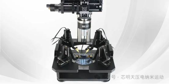
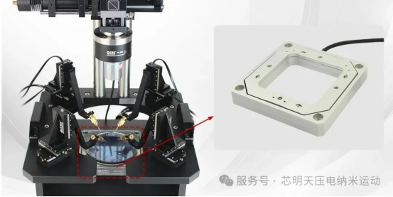
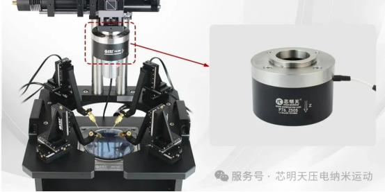
The Xinming piezoelectric nanoprobe stage consists of a piezoelectric nanopositioning stage, a piezoelectric motor displacement stage, a piezoelectric objective lens locator, and structural components. The piezoelectric nano positioning platform, as a sample bearing platform, can achieve two-dimensional high-precision deflection adjustment; fromThe probes controlled by four sets of piezoelectric motor displacement tables can achieve nanometer level precision motion in XYZ three-dimensional space; The piezoelectric objective lens locator achieves high-resolution microscopic observation by precisely controlling the objective lens to perform nanoscale focusing adjustment in the Z-axis direction.

1) Sample stand
The piezoelectric nano positioning platform can achieve single axis or even multi axis precision motion, with a motion range of up to millimeter level. It has the characteristics of small volume, no friction, and fast response speed. Equipped with high-precision sensors, it can achieve nanometer level resolution and positioning accuracy; The design features of high rigidity and zero clearance ensure the stability and repeatability of the system during operation, making it a reliable platform for carrying samples.

2) Probe station
The piezoelectric motor displacement table is driven by piezoelectric ceramics and designed with a special mechanical structure to convert the linear micro displacement generated by piezoelectric ceramics into macroscopic linear (or angular) motion of the mechanical plane, with a stroke of up to tens of millimeters (or360 °). The nanoscale repetitive positioning characteristics enable it to achieve high-precision positioning of probes. In response to the demand for controlling the force exerted on the sample by the probe, the Xinming piezoelectric motor displacement table provides nanoscale motion control and precise force output, providing accurate positioning and navigation for the probe's movement.

3) Microscopic focusing
When operating on microscopic samples such as biological cells, it is necessary to maintain both the clarity of sample observation and the accuracy of probe operation. The Xinming piezoelectric objective lens locator is specially designed for objective focusing microscopy, using a flexible hinge parallel guiding mechanism without hysteresis. The object lens compensation is small and has ultra-high focusing stability. The objective lens locator is installed in microscopic detection/Measurement or observation devices can be equipped with animal microscopes to improve accuracy, and can be used in conjunction with various high-resolution microscopes to achieve nanoscale collaborative positioning of samples and optical systems.

The probe station shown in the figure integrates multiple piezoelectric products from Xinmei, and its core configuration includes:S54 2D swing table, which can flexibly customize parameters according to actual needs; The N56 series linear motor displacement table has a rich range of stroke options, with a maximum stroke of over 50mm; Piezoelectric objective lens locator, multi stroke optional, with a maximum resolution of 2.5nm.
2. Nineteen dimensional piezoelectric nanoprobe stage: integration of micro nano operations
The Xin Tomorrow piezoelectric nanoprobe station is a nanoprobe station that combines a piezoelectric nanopositioning station and a nanoprobe module based on a piezoelectric motor displacement station. It can be used with scanning electron microscopy(SEM)、 Transmission electron microscopy (TEM) and other electron microscopes are used in conjunction for nanoscale manipulation. The central sample stage can perform XYZ three-axis motion, and four sets of nano probe modules can perform XYZ three-dimensional linear and R-axis rotational motion. The external dimensions, motion axis, stroke, and speed parameters of the nanoprobes can be customized.

| Piezoelectric nanoprobe stage | |
| Nano probe station | |
| Degree of freedom in motion | XYZ |
| Z-resolution | ≤2nm |
| Z-direction travel | ≥20μm |
| XY itinerary | ≥20mm |
| XY velocity | ≥30mm/s |
| Nano probe module | |
| Degree of freedom in motion | X. Y, Z three-dimensional straight lines and R axis rotation |
| XYZ directional positioning resolution | ≤100nm |
| XY direction travel | ≥5mm |
| Z-direction travel | ≥0.5mm |
| R-direction travel | 180° |
| Scanning resolution | ≤2nm |
| Usage environment | |
| Use vacuum degree | achievable10^-4Pa |
| Temperature range for use | -45 ℃ to 100 ℃ |
| Parameters can be customized | Various parameters such as external dimensions, fixed interfaces, motion axis, stroke, speed, etc. can be customized |
For more details, please call Xin tomorrow!