-
E-mail
zhxuanjun@189.cn
-
Phone
13916501195
-
Address
Room 917, Building 10, No. 77 Futexi 3rd Road, Pudong New Area, Shanghai
Shanghai Zhengheng Electronic Technology Co., Ltd
Detailed introduction to the technical characteristics of IC high-frequency near-field scanner
Date: 2025-08-12Read: 5
IC high-frequency near-field scanner is an important tool for detecting electronic components and circuit boards. By utilizing the interaction between high-frequency signals and target objects to obtain information, it is widely used in integrated circuit (IC) testing, fault diagnosis, and quality control of electronic products. It mainly relies on the principle of interaction between high-frequency electromagnetic waves and the measured object for operation. Specifically, it applies electromagnetic waves of a certain frequency to the circuit by contacting or approaching the surface of the circuit through a near-field probe, and detects reflected or transmitted signals. Based on the changes in the reflected signal, the electrical characteristics and fault location of the circuit can be inferred.
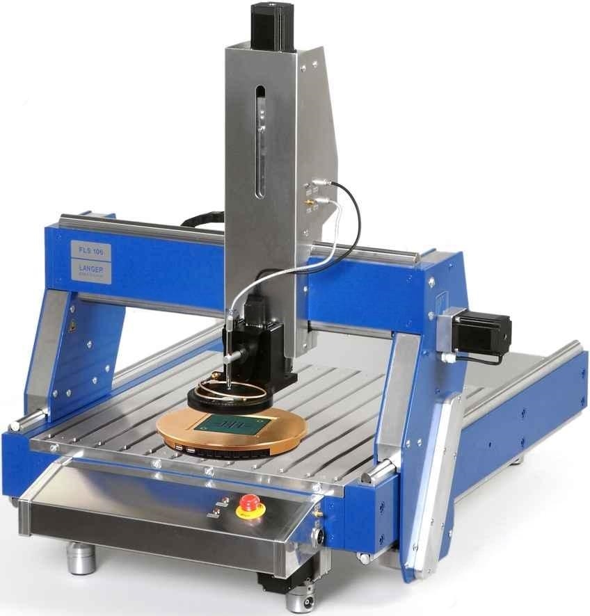
IC high-frequency near-field scannerTechnical features:
1. High precision testing
High frequency near-field scanners can accurately measure high-frequency signals in circuits, which is particularly important for small-sized integrated circuits. During the testing process, the near-field probe can directly contact or approach the test area, avoiding far-field interference and thus improving the testing accuracy.
2. Wide frequency range
High frequency near-field scanners typically have a wide operating frequency range, covering signal frequencies from a few GHz to tens of GHz, to meet the testing needs of different electronic components and circuit boards.
3. Real time data collection
The high-frequency near-field scanner is equipped with advanced data acquisition technology, which can provide real-time feedback on test results. This enables engineers to quickly locate problems and make adjustments, thereby improving work efficiency.
4. Automated scanning and positioning
Many high-frequency near-field scanners have the functions of automated scanning and fault location. With the support of intelligent software, the system can automatically scan the circuit board and identify potential fault areas, reducing the complexity of manual operations.
Application scenarios of IC high-frequency near-field scanner:
1. Quality control of integrated circuits (ICs)
As the core of modern electronic products, the quality control of integrated circuits is crucial. Detailed testing can be conducted on the electrical characteristics inside the IC to ensure the stability of the product during high-frequency operation.
2. PCB (Printed Circuit Board) inspection
In the production process of PCB, small circuit board defects or design issues are often encountered. High frequency near-field scanners can help quickly locate these issues and ensure that the quality of the circuit board meets standards.
3. Fault diagnosis
Electronic products often experience malfunctions during use, which may be caused by damaged components, poor soldering, or design issues. By scanning the high-frequency signals of the circuit board, engineers can identify the specific location of faults and quickly repair them.
4. High frequency circuit testing
High frequency circuits, such as radio frequency (RF) circuits and high-speed digital circuits, typically require high-precision testing tools. Being able to effectively detect the signal integrity, power distribution, and other electrical characteristics of these circuits is an important tool for high-frequency circuit design verification.