-
E-mail
zhxuanjun@189.cn
-
Phone
13916501195
-
Address
Room 917, Building 10, No. 77 Futexi 3rd Road, Pudong New Area, Shanghai
Shanghai Zhengheng Electronic Technology Co., Ltd
PCB near-field scanner has the advantages of fast detection and real-time feedback
Date: 2025-08-17Read: 7
PCB near-field scanner is a device used for analyzing and detecting PCB performance, widely used in the fields of electronic design, testing, and manufacturing. It utilizes scanning technology to perform high-resolution imaging of the surface and inner layers of circuit boards, in order to detect anomalies, short circuits, open circuits, and other potential issues in the circuits.
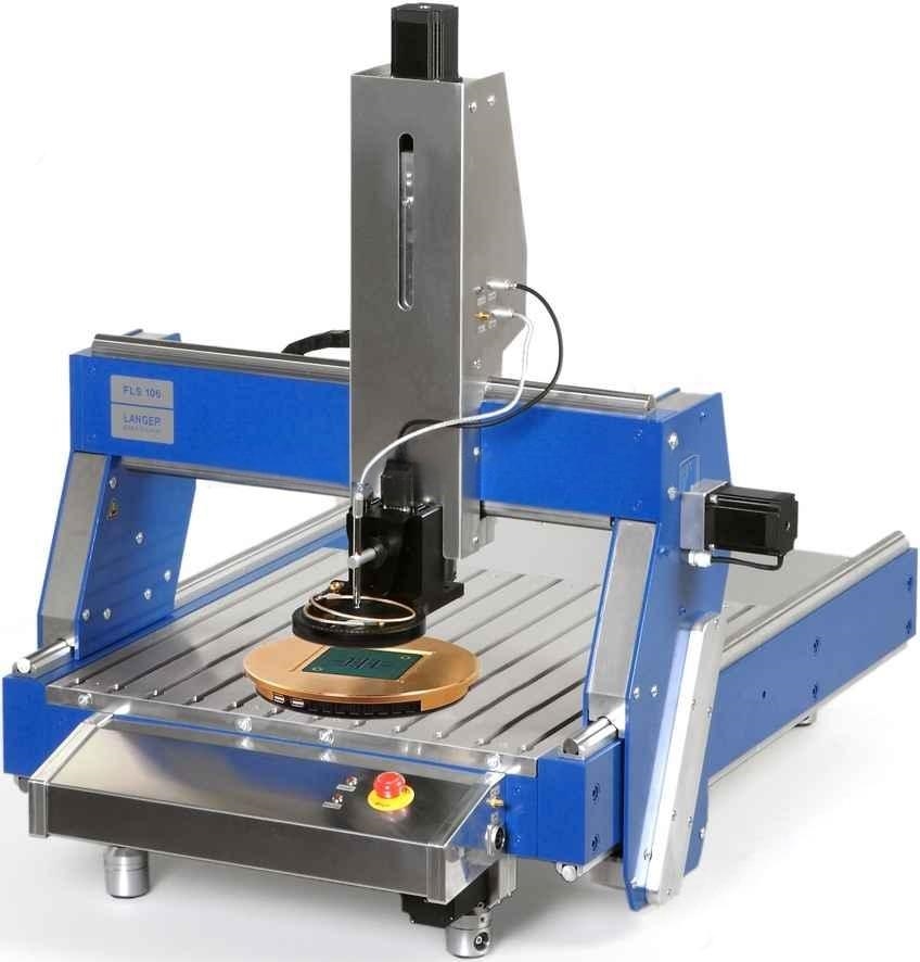
PCB near-field scannerWorking principle:
1. The function of scanning probes
Using a special scanning probe that can be very close to the surface of the circuit board and detect signals on the circuit board through weak electromagnetic field changes. These signals may be related to the transmission of current, impedance changes, or electrical noise.
2. Interaction between probes and circuits
The probe usually moves along the set path on the PCB surface to collect signals from each point. By detecting changes in current or voltage fluctuations on the board, near-field scanners can identify potential issues with the circuit board, such as signal attenuation and noise interference.
3. Data analysis and imaging
The collected data will be transmitted to a computer system and processed to form two-dimensional or three-dimensional images. Users can visually see the performance issues of the circuit board on the images, which can help engineers quickly locate the faulty area for repair or optimization design.
Advantages of PCB near-field scanner:
1. High precision and high resolution
Compared with traditional detection methods, near-field scanners can provide higher resolution and accuracy, especially suitable for PCB boards with small sizes and complex structures. This enables it to detect subtle signal changes and circuit defects.
2. Non destructive testing
The near-field scanner adopts a non-contact detection method, which can perform comprehensive scanning and diagnosis without damaging the PCB. This is particularly important because for complex and expensive circuit boards, any physical damage can result in significant losses.
3. Rapid detection and real-time feedback
The near-field scanner can complete high-precision scanning in a short period of time and is suitable for real-time detection of circuit boards in large-scale production processes. In this way, quality issues on the production line can be quickly reported to engineers, avoiding problems in mass production.
4. Multi functional integration
Modern near-field scanners typically integrate multiple functions such as electromagnetic radiation testing, signal integrity analysis, thermal imaging, etc., enabling them to provide more comprehensive data support when detecting PCBs.