-
E-mail
dmsci@vip.163.com
-
Phone
021-56654814
-
Address
707-709A, Science and Technology Building, Shanghai University Science and Technology Park, 788 Guangzhong Road, Jing'an District, Shanghai
Product Categories
Shanghai Dumei Precision Instrument Co., Ltd

High resolution thermal field emission scanning electron microscope
NegotiableUpdate on 03/17
- Model
- Nature of the Manufacturer
- Producers
- Product Category
- Place of Origin
Overview
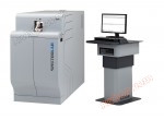
Verios XHRSEM Verios is the second generation product of FEI's leading XHR (high-resolution) SEM series
Product Details
Verios XHR SEM
VerioscorrectFEIleadingXHR(High resolution)SEMThe second generation product of the series. In cutting-edge semiconductor manufacturing and materials science applications, it can 1 to30 kVProvide sub nanometer resolution and enhanced contrast within the range, meeting the requirements of precision material measurement without weakening traditional scanning electron microscopes(SEM)High throughput, analytical capabilitiesAdvantages such as sample flexibility and ease of use.
VeriosThe Application of Materials Science
For material scientists,VeriosSub nanometer characterization can be extended to newly developed materials such as catalyst particles, nanotubes, pores, interfaces, biological objects, and other nanoscale structures, enabling them to make important new discoveries. No need to switch to usingTEMHigh resolution and high contrast images can be obtained using other imaging techniques.VeriosIt can be flexibly used for various research applications and can accommodate large samples such as full-size wafers or metallurgical samples. You can perform rapid analysis in high current mode and also carry out precise prototyping applications, such as electron beam induced material direct deposition or photolithography.
Excellent low voltageSEMResolution and material contrast
VeriosIntended to increase the publishable output of your laboratory.VeriosYou can500 eVarrive30 keVThe sub nanometer resolution within the complete energy range is extended to new materials such as catalyst particles, nanotubes, pores, interfaces, biological objects, and other nanoscale structures. No need to switch to usingTEMHigh resolution and high contrast images can be obtained using other imaging techniques.VeriosIt can be flexibly applied to various research applications and can accommodate large samples such as full-size wafers or metallurgical samples. You can perform rapid analysis in high current mode and also carry out precise prototyping applications, such as electron beam induced material direct deposition or photolithography.
Exploring High ResolutionSEMThe world presented
VerioscorrectFEIleadingXHR SEMThe second generation product of the series, through 1 arrive30 kVProvide accurate imaging with sub nanometer resolution within the energy range. It can provide excellent contrast required for precise measurement of materials in various application fields without affecting high-throughput, analytical functionality, sample flexibility, and traditional methodsSEMThe ease of use.VeriosFeaturing unique technologies such as constant power lenses that enhance thermal stability and electrostatic scanning that improves deflection linearity. It is very flexible in selecting parameters, processing large samples, or supporting more applications such as analysis or lithography. with the help ofVerios XHR SEMBoth temporary users and experts can obtain accurate and complete nanoscale data in a short period of time, discovering information that was previously unavailable using other technologies.
Similar Product Recommend